Frostbite CPU: What the AI-Designed Chip Claims Really Show
Frostbite CPU is Architect Labs' AI-designed chip architecture. See what the 4.59x perf-per-watt claim compares, what is pre-silicon, and what to verify next.
Contents7 sections
Key takeaways
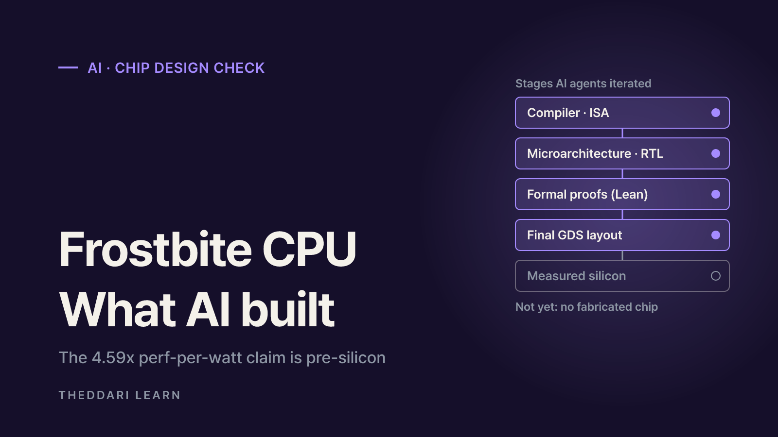
- Frostbite CPU is an experimental architecture announced by Architect Labs on November 18, 2026; the company says AI agents iterated on its compiler, ISA, RTL, verification and final GDS.
- The headline 4.59x is a geometric-mean performance-per-watt figure against one undisclosed dual-issue, in-order core; on the 15 held-out workloads it is 3.83x.
- As of November 21, 2026 there is no fabricated chip, no announced product and no independent replication; results come from 7 nm synthesis and layout.
- Releasing the RTL and ISA, an FPGA playground and SPEC/PARSEC benchmarks are stated plans, so treat the numbers as company claims until they arrive.
Frostbite CPU is an experimental general-purpose processor architecture that the US startup Architect Labs unveiled on November 18, 2026. The company says swarms of AI agents designed and verified it end to end, from a brand-new instruction set through RTL to a final GDS layout, and that it delivers 4.59x the performance per watt of a conventional CPU core. As of November 21, 2026, those results are pre-silicon estimates, the comparison core is unnamed, and nothing has been independently reproduced. This guide separates what the original announcement claims the AI did, how the headline numbers were produced, and what remains unverified.
What is Frostbite CPU? An interaction-net processor
Frostbite is built around interaction nets, a model of computation introduced by Yves Lafont in 1990. A program is a graph of nodes, and computation proceeds by rewriting connected pairs of nodes. Each rewrite touches only a small local part of the graph, and active pairs never overlap, so they can be reduced in any order or all at once with the same result. Every value is used exactly once, which means there is no shared mutable state for hardware to guard.
Conventional CPUs spend large amounts of area and power rediscovering dependencies at runtime with out-of-order machinery, deep caches and coherence protocols. Frostbite instead uses a grid of small tiles, each with its own local memory. Programs are written in Vine, a language with Rust-like syntax, and compiled to an intermediate representation called Ivy. There is no central scheduler: a tile runs its own work first, takes spare work from a neighbor when idle, and otherwise goes inactive to save power. Architect Labs says no human specified this work-stealing behavior; the agents arrived at it while fixing performance regressions.
Is the idea new?
Not entirely. Dataflow hardware and graph reduction have long research histories. In the Hacker News thread, commenters pointed to WaveScalar and to the HVM runtime used by the Bend language, and several argued that the real barrier for such designs has always been the cost of porting existing software. The novelty Architect Labs emphasizes is the process: agents carrying an unusual computing model all the way to a chip layout.
AI chip design claims: what the agents did and what people set up
Reading the announcement carefully, the division of labor looks like this. People defined 25 workloads across five categories (parallel, staged, sequential, branching and recursive) and split each category into a search set used for tuning and a held-out set reserved for final evaluation. They also built an in-house specification language called ASL, a system model called Arcmodel, and a flow that translates specifications into Lean for theorem proving. Inside that frame, agent swarms compared architectures, wrote RTL, recalibrated power models and kept or dropped ideas.
Workload choice
- What the company reports
- Humans picked 25 workloads and the split
- What to keep in mind
- SPLASH-2-style kernels ran 64x smaller than usual
Exploration
- What the company reports
- Agents wrote a 141-page architecture draft
- What to keep in mind
- Draft was deleted after first RTL; its estimates were far off
Spec and proofs
- What the company reports
- ASL contracts lowered to 800k+ lines of Lean
- What to keep in mind
- Public material does not show which properties are proven
Iteration
- What the company reports
- 58 ideas tried, 37 kept over four searches
- What to keep in mind
- Selection criteria and failures are not detailed
Physical design
- What the company reports
- 800 MHz at synthesis, 500 MHz in final GDS
- What to keep in mind
- No fabricated or measured silicon
So "designed and verified by AI" is best read as agents rapidly exploring and implementing a design space inside human-built problem definitions and verification tooling. One Hacker News commenter put it as AI synthesizing decades of research ideas into an engineered product. Another asked the right question about formal verification: does the proof correspond to the chip, and does it prove properties that matter? Answering that needs the promised ASL write-up and RTL release.
How to read the 4.59x performance-per-watt figure
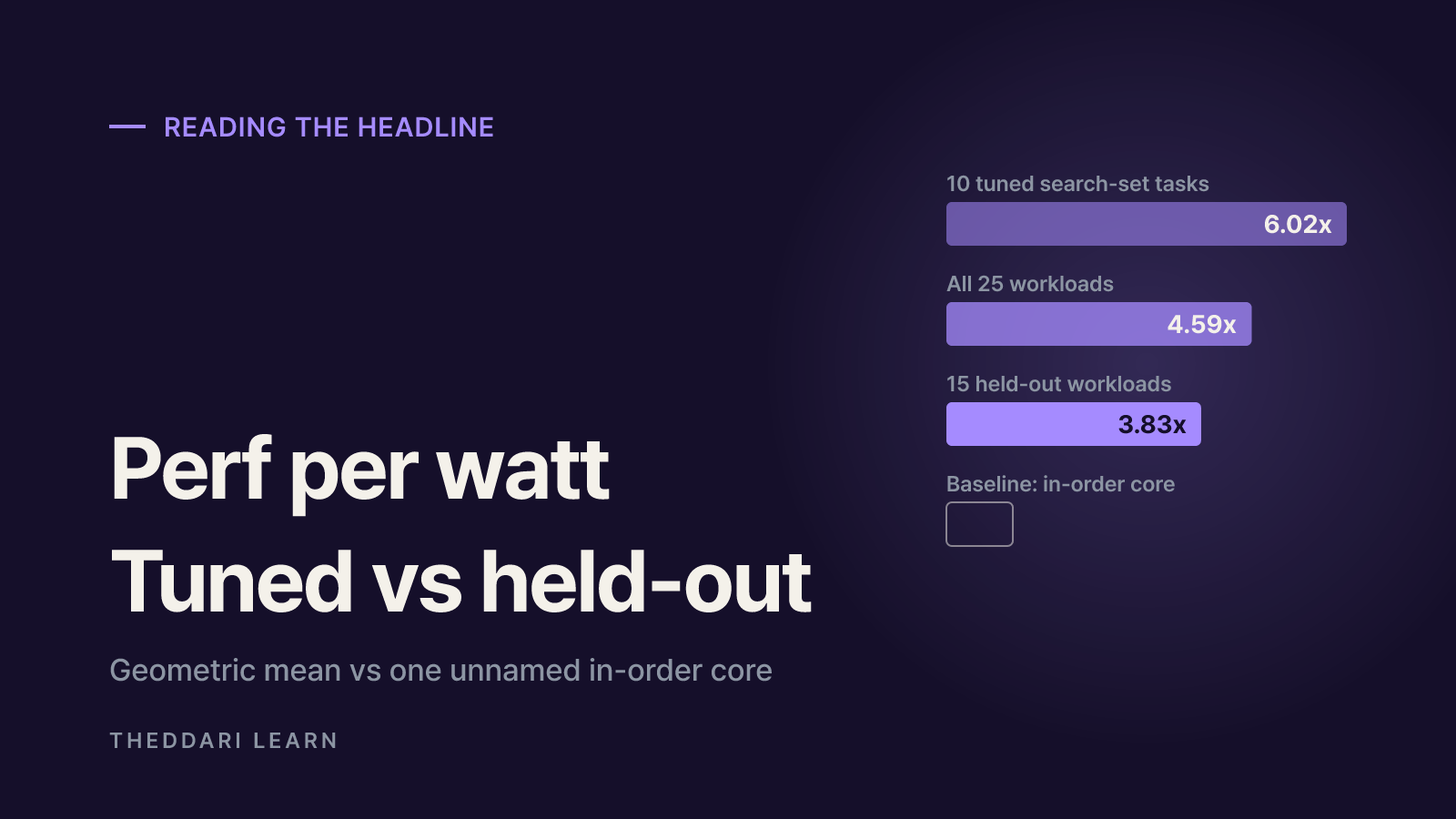
The headline is a geometric mean of 4.59x performance per watt across all 25 workloads. The unit being compared is one Frostbite quad (a 2x2 group of tiles plus four L3 nodes, 0.792 mm²) against one core of a conventional CPU, called TCPU, which measures 0.895 mm² on the same 7 nm process. Performance per area averages 8.77x. Split the mean apart and the picture changes: 6.02x on the 10 search-set workloads the agents tuned against, and 3.83x on the 15 held-out workloads.
- Tuned versus held-out: The gap between 6.02x and 3.83x suggests some fitting to familiar workloads. The held-out 3.83x is the better estimate of generalization.
- The baseline: A dual-issue, in-order core whose identity is withheld "for legal reasons." It is not a wide out-of-order core of the kind found in laptops and servers.
- Efficiency, not speed: Performance per watt says nothing directly about absolute speed. The final layout runs at 500 MHz.
- Wide spread: Per-workload results range from 23.12x on conv2d to 1.15x on recursive Fibonacci, and the company says the design is strongest on highly parallel work.
- Where energy goes: Excluding clock distribution, memory falls from 57% of TCPU energy to 38%, and fetch/decode/issue from 27% to 6%, but the on-chip network and scheduler add 26%.
Commenters disagreed about the baseline. Some called an in-order core a weak target; others noted that for a perf-per-watt comparison, efficient in-order cores are actually the tougher rival. Architect Labs says it will benchmark against multicore and larger out-of-order CPUs on SPEC and PARSEC in the coming months, which is the evidence that would settle the argument.
What is still unverified
As Notebookcheck noted, Frostbite is an experimental architecture rather than a production processor. As of November 21, 2026, public material does not establish the following:
- Silicon results: Power and performance come from synthesis and layout flows. The company itself calls them pre-silicon numbers that need tape-out loops to correlate with real measurements.
- Independent replication: The RTL and ISA have not been released, so outside researchers cannot reproduce the results.
- Real software: Programs must be written in Vine. There is no evidence yet on operating systems, databases, browsers or compilers.
- Scaling: A 4x4 array kept a similar power breakdown, but head-to-head multicore comparisons are still planned.
- Engineering savings: The post does not quantify engineer hours, compute cost or how much human review the agents needed.
Headlines framing Frostbite as an AI CPU that beats Intel and AMD overstate the source. The published comparison is an efficiency ratio against one small in-order core, not a performance test against shipping desktop or server processors.
A checklist for evaluating AI-designed chip announcements
More announcements built around AI chip design are likely. Running through the steps below helps separate marketing language from verified facts. If you track how AI tech stories spread, the theddari AI Telegram trends and blog trends pages show what is getting attention, though popularity is not evidence that a technical claim is true.
- 1
Locate the design stage
Find whether the work stopped at simulation, RTL, synthesis, GDS, tape-out or measured silicon. A GDS file is still not a measured chip.
- 2
Write down the baseline and metric
Record the comparison CPU's name, generation and core count, and whether the metric is raw performance, performance per watt or per area. Note the averaging method.
- 3
Separate tuning data from evaluation data
Read held-out results on their own and check whether workloads were scaled down for convenience.
- 4
Split AI work from human work
Identify who defined the problem, the evaluation criteria and the verification tools, and how much the agents decided on their own.
- 5
Check reproducibility
Look for released RTL, ISA documentation, benchmark code, standard benchmarks such as SPEC and third-party testing. Without them, file the result as a company claim.
 theddari.comTrendsBlog PostsSummarized Naver blog posts
Frostbite CPU is a notable case of AI agents, guided by formal specifications and proof tooling, carrying an unconventional computing model to a complete chip layout. The 4.59x figure, however, blends tuned and held-out workloads, rests on an unnamed small core, and has no silicon measurement or outside replication behind it yet. The most accurate way to read the announcement is to revisit it when the promised RTL and ISA release, FPGA playground and SPEC/PARSEC results appear.
Frequently asked questions
Is Frostbite a real chip I can buy?
Did AI really design a CPU without humans?
Does 4.59x mean Frostbite is 4.59 times faster than Intel or AMD CPUs?
How is this different from earlier dataflow CPUs?
Sources and references
- 1Architect Labs: Introducing Frostbite (Nov 18, 2026)(opens in a new tab)architectlabs.com
- 2Hacker News discussion thread(opens in a new tab)news.ycombinator.com
- 3Notebookcheck: AI designed an all-new CPU (Nov 20, 2026)(opens in a new tab)www.notebookcheck.net
- 4The Vine Programming Language(opens in a new tab)vine.dev
Related articles
 AI
Tencent Hy4-flash: Specs, API Cost, and Local Setup
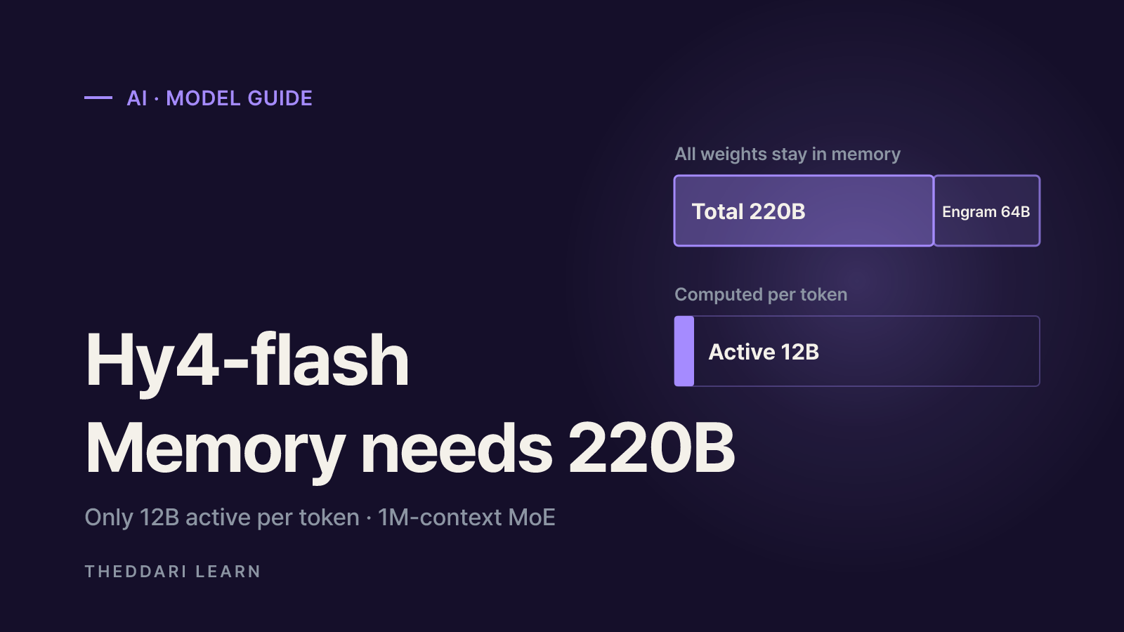
What Tencent's open-weight Hy4-flash actually is (220B total, 12B active, 1M context), how to read its in-house benchmarks, what the OpenRouter API costs, how much memory local GGUF and vLLM setups need, and when the Tencent Hy License requires a separate deal. Checked November 20, 2026.
 AI
Haru-4B Explained: Full-Duplex Voice Model and Local Setup
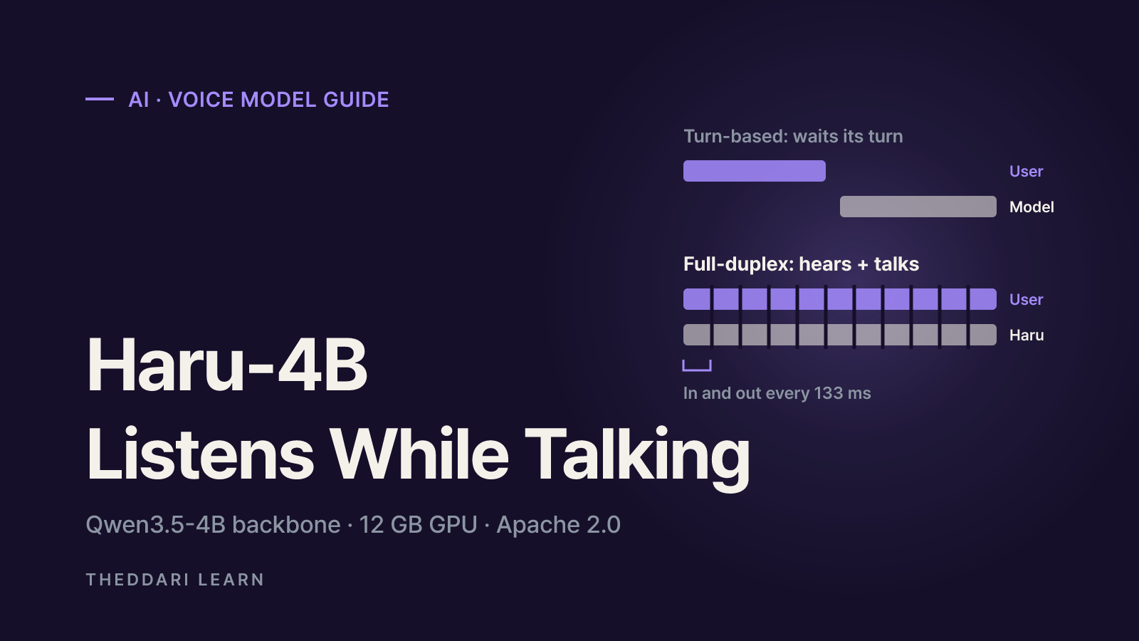
Haru-4B, the top trending model on Hugging Face, is not a small text chatbot. It is an open speech-to-speech base model that listens and speaks at the same time. Here is how it works, what hardware it needs, and what to check before running it.
 AI
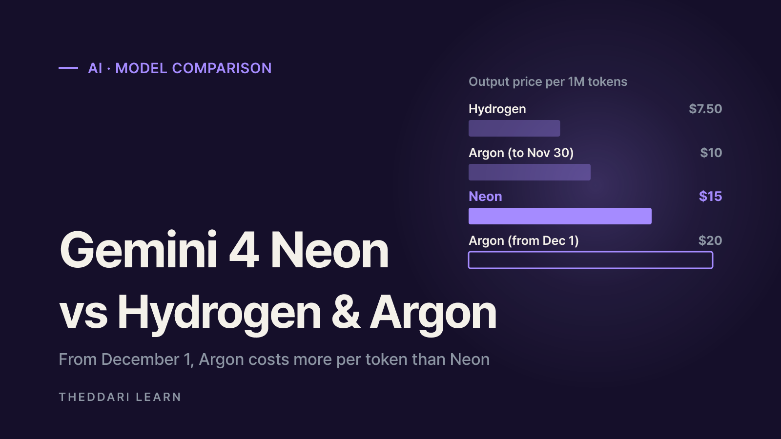
Gemini 4 Neon: Pricing, Access and Hydrogen vs Argon
Gemini 4 Neon is Google's new mid-tier Gemini 4 model, priced at $3 input and $15 output per million tokens with no free tier. Here is what Google announced, how it stacks up against Hydrogen and Argon, and what to check before you switch.